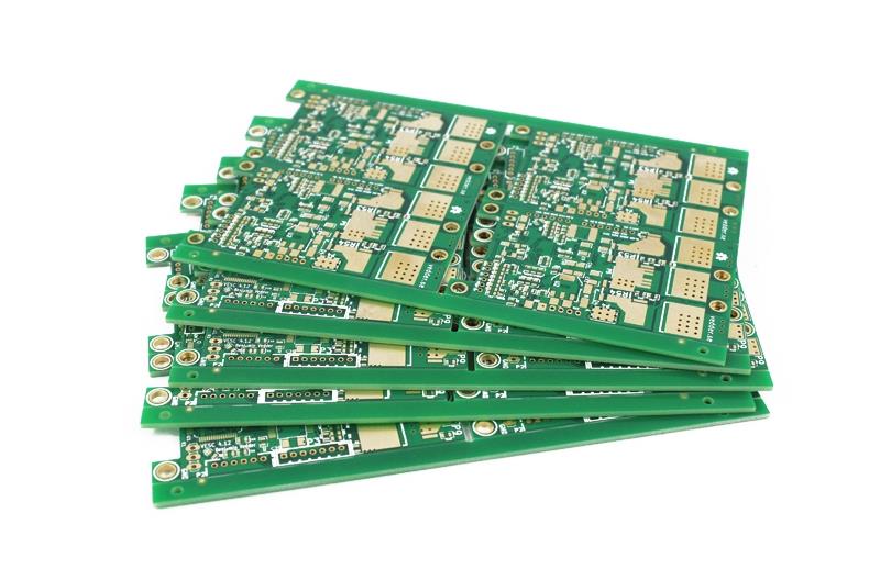
Q1: Why is gold plating used on PCBs?
Gold plating serves multiple crucial purposes on PCBs. Its exceptional conductivity, anti-oxidation properties, and durability make it ideal for connecting components, ensuring reliable signal transmission, and resisting corrosion over time.
Q2: What role do “gold fingers” play in PCBs?
“Gold fingers” serve as connectors between memory modules and their respective slots. These connectors, due to their gold plating, ensure efficient and reliable signal transmission, maintaining connectivity and integrity within electronic devices.
Q3: Why has gold plating been replaced by tin plating in some electronics?
The high cost of gold led to the adoption of tin plating in various consumer electronics since the 1990s. Tin, being more cost-effective, became the preferred choice for connectors in many devices, with gold remaining exclusive to high-performance servers and workstations due to its superior conductivity.
Q4: How does gold plating aid in high-density PCBs?
Gold plating provides smoother solder pads, crucial for the precision demanded by high-density PCBs. Its even surface ensures quality soldering, especially with ultra-small components, ultimately enhancing the overall soldering quality.
Q5: What drawbacks prompted the shift to immersion gold-plated PCBs?
As wiring became denser in PCBs, issues like signal distortion due to skin effect arose in multi-layered boards. To counter this, immersion gold plating emerged, offering benefits like improved soldering, reduced signal interference, and enhanced reliability due to its distinct crystal structure and signal transmission through copper layers.
Q6: How do immersion gold-plated PCBs differ from traditional gold plating?
Immersion gold plating presents a more yellow hue and improved soldering capability compared to traditional gold plating. Additionally, its crystal structure reduces oxidation, minimizes micro-shorts caused by gold wires, and ensures stronger adhesion between circuits and solder masks.
Q7: Are there other surface treatment options besides gold plating?
Certainly! Surface treatment methods include silver plating, OSP, and tin spraying (with or without lead), catering to specific material requirements. Each method has its merits and demerits, with considerations for storage conditions, soldering effectiveness, and material stability.
Q1: How does Mentor’s PCB design software handle differential lines?
A: After defining the differential pair properties, Mentor software allows routing two differential pairs together while strictly ensuring line width, spacing, and length matching. It can automatically separate them in case of obstacles and offers options for via connections during layer changes.
Q2: On a 12-layer PCB with three power layers (2.2V, 3.3V, 5V), how should the ground be handled?
A: Generally, assigning each power to a separate layer improves signal quality as it reduces the likelihood of signal crossing plane separations, a crucial factor affecting signal quality. Additionally, power plane coupling and symmetrical layer stacking need consideration.
Q3: How do PCB manufacturers check if the manufactured PCB meets design requirements?
A: PCB Manufacturers like these conduct network continuity tests by applying power before finalization. X-ray tests are increasingly used to inspect etching or lamination faults. ICT (In-Circuit Testing) examines finished PCBs with added test points during design. In case of issues, special X-ray examination can identify manufacturing-related faults.
Q4: Is “mechanical protection” equivalent to shielding in a device’s casing?
A: Yes, ensuring the device casing is tightly sealed and minimizes the use of conductive materials while maximizing grounding is vital for protection.
Q5: When selecting chips, should one consider the chip’s ESD characteristics?
A: It’s essential to consider a chip’s ESD characteristics during selection. These details are often mentioned in the chip specifications, and the performance of similar chips from different manufacturers can vary. Comprehensive considerations during design can guarantee improved circuit board performance.
Q6: Should the ground form a closed loop for reduced interference during PCB design?
A: PCB design aims to minimize loop areas to reduce interference. Ground lines shouldn’t form closed loops; instead, a branching tree-like structure is preferred while maximizing ground area.
Q7: When using a separate power source for a simulator and a PCB, should their ground be connected?
A: While separate power sources can reduce interference, specific device requirements might necessitate connecting their grounds. Ideally, if the simulator and PCB use distinct power sources, shared grounding might not be advisable.
Q8: Should multiple PCBs constituting a circuit share a common ground?
A: Typically, multiple PCBs constituting a single circuit should share a common ground, as using multiple power sources practically might not be feasible. However, reducing interference might be somewhat limited.
Q9: How can ESD testing be passed for a handheld product with a metal casing, LCD, and CPU operating at 33MHz?
A: For a handheld product with a metal casing, ESD-related issues might be significant. If the metal material cannot be changed, adding anti-static materials internally and strengthening PCB grounding while finding a way to ground the LCD might help, though specific solutions would depend on the actual conditions.
Q10: In designing a system with DSP and PLD, what ESD aspects should be considered?
A: ESD protection measures should primarily focus on parts in direct contact with humans, providing appropriate protection both in the circuits and the device structure. The degree of ESD impact on a system varies based on environmental factors and system sensitivity, thus requiring attention and preventive measures during design.